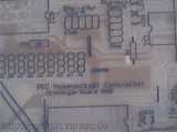
This gallery shows my two trials at the PCB for the PIC Homecockpit Controller Motherboard.
Both trys used the same technique, the toner transfer method, but due to the failure of my first try, I changed a couple of variables, like iron temperature, pressure and pressing time. The second try worked very nicely, as you will be able to see.
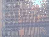
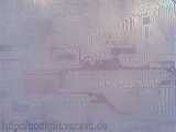
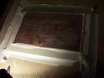
To start off, here are a few pics of the failed first try... the picture above shows the board after soaking (you can see from the reflections that it indeed IS soaked :) and peeling/rubbing off pieces of the paper...
a little closer so we can see the area where I started to rub off the soaked paper.
...and closer. Seen here are the power connector pads where one of these floppy power connectors will go. The toner proved to be holding on to the copper really well. I used the highest setting (linen) on the iron and applied a good amount of pressure. The time was probably about 2-3 minutes.
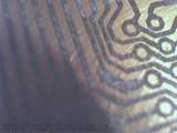
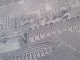
One of the high density area. This is where the keymatrix daughterboard connectors will go. Thats 14 wires/traces going parallel between 2x7 pinheaders. A little hard to see, but the traces got flattened out from the heat and pressure and now make contact to neighboring pads :(
In case you are wondering about the paper type: Its Reichelt Catalogue paper again, which works reasonably well, but any type of smooth surface/glossy catalogue or advertisement paper works.
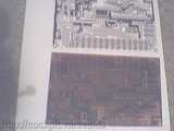
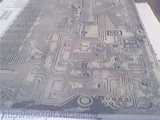
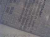
After peeling off all paper, comparing with a printout on normal paper
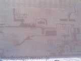
About the only area where the toner came off. That wouldn't have been a problem...
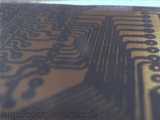
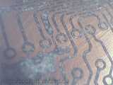
...however, this was a problem: lots of traces molten together. This picture shows how some traces are thicker/flatter than others
A closeup of the problem area
Here starts the second part of the gallery with my second try at this PCB using the toner transfer method.
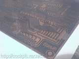
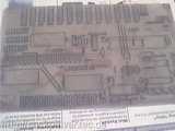
This time nearly the whole board was perfect... just a few things I had to correct by hand.
Note that this board has a couple of places where there are traces with a width of 12mils (0.012inches) and also spaced 12mils.
Most of the rest of the board is routed with standard 16mil traces.
This is the hardest area with the mentioned 12mils traces/spaces. Compare this to the first version in picture #8.
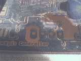
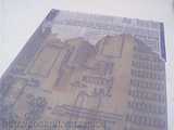
This was the biggest problem with the second try. Due to irregularities in the PCB material, this part (socket for the serial port) did not tranfer fully.
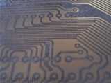
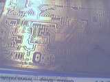
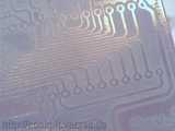
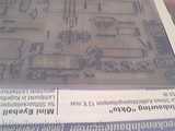
Another area where the first try just melted together those three 12 mil traces into one big blob. As you can see, it worked very nice this time.
12 mil traces with 12 mil spaces, traces between two IC pads... no problem this time
Trying to fix the serial port part. I wanted to see if I could just iron this piece again... which did not work out very well. Also, lining up is very hard to do just right. I assume that the reason the newly ironed on toner didn't stick is that the copper wasn't clean enough... So I ended up...
Drawing the traces with a water resistant pen and the used Seno rub-on tranfer lettering for the pads.
After etching... (I used FeCl3 this time)
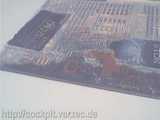
Checking the problem areas... You can see where I improvised little things with the pen
After removing the toner (and ink from the pen). Toner removal seems to be the hardest part... I used fine sandpaper this time.
The light shows the direction I used the sandpaper on the board
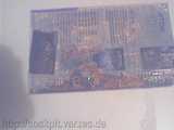
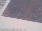
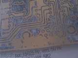
Overall look is OK.
Again, checking the 12mil traces/spaces
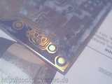
The component side. Ready for my component print... of course using toner transfer :-)
After ironing on and soaking in water...
I took less care when doing the component side. If its messed up... oh well. It does not hinder functionality.
Here is the area for the pinheaders for the analog channels. (Seen through the paper)
Removing the paper... came off very easily in big pieces.
All paper removed. I wanted to see if I could seal the print with spray plasic (Its called "Plastik 70" from Kontakt Chemie/CRC Industries). A nice side effect is that the paper fibers that stayed on the toner are not visible as they are when the water drys out because the spray plastic makes them wet and then drys off from the surface, but leaving the fibers "invisble".
However, there is a problem with the plastic spray that I noticed when trying to "shake off" excess liquid plastic after spraying. The spray seems to solve the toner as parts "swam away" as seen on the follwing pictures.
The "swimming away" effect where toner layers moved when I shook the board with the still wet spray plastic.
Closup of the component print. Even with the swimming away, it looks decent :-)
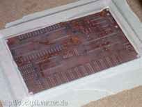
After drilling the PCB using our homebuilt XYZ table (not under computer control, but rather using four eyes and four hands)
The board has over 400 holes, so this took a while, but is definately worth the effort. We did not break a single drill, even though we used 0.6mm and 0.8mm for most holes.
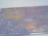
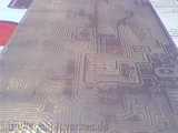
I don't know why the copper came out with this weird reddish color on the digital camera.
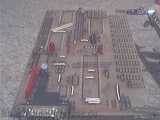
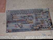
Overall view.
Closeup
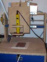
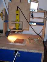
The machine.
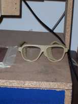
Eyes are expensive these days, so we use protective glasses in case a drill breaks and tries to make its way to the nearest human eye :-)
Good lighting is important for such detailed work
The result from the component side
Adding components. Serial port on the lower left corner, PIC will go into the 40 pin IC placeholder, Keymatrix daughterboards will go along the right and upper border.